 | –≠–ª–µ–∫—Ç—Ä–æ–Ω–Ω—ã–π –∫–æ–º–ø–æ–Ω–µ–Ω—Ç: DS90LV017 | –°–∫–∞—á–∞—Ç—å:  PDF PDF  ZIP ZIP |

DS90LV017A
LVDS Single High Speed Differential Driver
General Description
The DS90LV017A is a single LVDS driver device optimized
for high data rate and low power applications. The
DS90LV017A is a current mode driver allowing power dissi-
pation to remain low even at high frequency. In addition, the
short circuit fault current is also minimized. The device is de-
signed to support data rates in excess of 600Mbps
(300MHz) utilizing Low Voltage Differential Signaling (LVDS)
technology.
The device is in a 8-lead small outline package. The
DS90LV017A has a flow-through design for easy PCB lay-
out. The differential driver outputs provides low EMI with its
typical low output swing of 355 mV. The DS90LV017A can be
paired
with
its
companion
single
line
receiver,
the
DS90LV018A, or with any of National's LVDS receivers, to
provide a high-speed point-to-point LVDS interface.
Features
n
>
600 Mbps (300 MHz) switching rates
n
0.3 ns typical differential skew
n
0.7 ns maximum differential skew
n
1.5 ns maximum propagation delay
n
3.3V power supply design
n
±
355 mV differential signaling
n
Low power dissipation (23 mW
@
3.3V static)
n
Flow-through design simplifies PCB layout
n
Interoperable with existing 5V LVDS devices
n
Power Off Protection (outputs in high impedance)
n
Conforms to TIA/EIA-644 Standard
n
8-Lead SOIC package saves space
n
Industrial temperature operating range
(-40∞C to +85∞C)
Connection Diagram
Functional Diagram
TRI-STATE
Æ
is a registered trademark of National Semiconductor Corporation.
Dual-In-Line
DS100101-1
Order Number DS90LV017ATM
See NS Package Number M08A
DS100101-2
March 2000
DS90L
V017A
L
VDS
Single
High
Speed
Differential
Driver
© 2000 National Semiconductor Corporation
DS100101
www.national.com

Absolute Maximum Ratings
(Note 1)
If Military/Aerospace specified devices are required,
please contact the National Semiconductor Sales Office/
Distributors for availability and specifications.
Supply Voltage (V
CC
)
-0.3V to +4V
Input Voltage (DI)
-0.3V to +3.6V
Output Voltage (DO
±
)
-0.3V to +3.9V
Maximum Package Power Dissipation
@
+25∞C
M Package
1190 mW
Derate M Package
9.5 mW/∞C above +25∞C
Storage Temperature Range
-65∞C to +150∞C
Lead Temperature Range Soldering
(4 sec.)
+260∞C
ESD Ratings
(HBM 1.5 k
, 100 pF)
8kV
(EIAJ 0
, 200 pF)
1000V
(CDM)
1000V
(IEC direct 330
, 150 pF)
4kV
Recommended Operating
Conditions
Min
Typ
Max
Units
Supply Voltage (V
CC
)
3.0
3.3
3.6
V
Temperature (T
A
)
-40
25
+85
∞C
Electrical Characteristics
Over Supply Voltage and Operating Temperature ranges, unless otherwise specified. (Notes 2, 3, 7)
Symbol
Parameter
Conditions
Pin
Min
Typ
Max
Units
DIFFERENTIAL DRIVER CHARACTERISTICS
V
OD
Output Differential Voltage
R
L
= 100
(
Figure 1)
DO+,
DO-
250
355
450
mV
V
OD
V
OD
Magnitude Change
1
35
mV
V
OH
Output High Voltage
1.4
1.6
V
V
OL
Output Low Voltage
0.9
1.1
V
V
OS
Offset Voltage
1.125
1.2
1.375
V
V
OS
Offset Magnitude Change
0
3
25
mV
I
OXD
Power-off Leakage
V
OUT
= V
CC
or GND, V
CC
= 0V
±
1
±
10
µA
I
OSD
Output Short Circuit Current
-5.7
-8
mA
V
IH
Input High Voltage
DI
2.0
V
CC
V
V
IL
Input Low Voltage
GND
0.8
V
I
IH
Input High Current
V
IN
= 3.3V or 2.4V
±
2
±
10
µA
I
IL
Input Low Current
V
IN
= GND or 0.5V
±
1
±
10
µA
V
CL
Input Clamp Voltage
I
CL
= -18 mA
-1.5
-0.6
V
I
CC
Power Supply Current
No Load
V
IN
= V
CC
or GND
V
CC
5
8
mA
R
L
= 100
7
10
mA
Switching Characteristics
Over Supply Voltage and Operating Temperature Ranges, unless otherwise specified. (Notes 3, 4, 5, 6)
Symbol
Parameter
Conditions
Min
Typ
Max
Units
DIFFERENTIAL DRIVER CHARACTERISTICS
t
PHLD
Differential Propagation Delay High to Low
R
L
= 100
, C
L
= 15 pF
0.3
0.8
1.5
ns
t
PLHD
Differential Propagation Delay Low to High
(
Figure 2 and Figure 3)
0.3
1.1
1.5
ns
t
SKD1
Differential Pulse Skew |t
PHLD
- t
PLHD
| (Note 8)
0
0.3
0.7
ns
t
SKD3
Differential Part to Part Skew (Note 9)
0
1.0
ns
t
SKD4
Differential Part to Part Skew (Note 10)
0
1.2
ns
t
TLH
Transition Low to High Time
0.2
0.5
1.0
ns
t
THL
Transition High to Low Time
0.2
0.5
1.0
ns
f
MAX
Maximum Operating Frequency (Note 11)
350
MHz
Note 1: "Absolute Maximum Ratings" are those values beyond which the safety of the device cannot be guaranteed. They are not meant to imply that the devices
should be operated at these limits. The table of "Electrical Characteristics" specifies conditions of device operation.
Note 2: Current into device pins is defined as positive. Current out of device pins is defined as negative. All voltages are referenced to ground except V
OD
.
Note 3: All typicals are given for: V
CC
= +3.3V and T
A
= +25∞C.
Note 4: These parameters are guaranteed by design. The limits are based on statistical analysis of the device performance over PVT (process, voltage, temperature)
ranges.
Note 5: C
L
includes probe and fixture capacitance.
Note 6: Generator waveform for all tests unless otherwise specified: f = 1 MHz, Z
O
= 50
, t
r
1 ns, t
f
1 ns (10%-90%).
DS90L
V017A
www.national.com
2
Switching Characteristics
(Continued)
Note 7: The DS90LV017A is a current mode device and only function with datasheet specification when a resistive load is applied to the drivers outputs.
Note 8: t
SKD1
, |t
PHLD
- t
PLHD
|, is the magnitude difference in differential propagation delay time between the positive going edge and the negative going edge of the
same channel.
Note 9: t
SKD3
, Differential Part to Part Skew, is defined as the difference between the minimum and maximum specified differential propagation delays. This speci-
fication applies to devices at the same V
CC
and within 5∞C of each other within the operating temperature range.
Note 10: t
SKD4
, part to part skew, is the differential channel to channel skew of any event between devices. This specification applies to devices over recommended
operating temperature and voltage ranges, and across process distribution. t
SKD4
is defined as |Max - Min| differential propagation delay.
Note 11: f
MAX
generator input conditions: t
r
= t
f
<
1 ns (0% to 100%), 50% duty cycle, 0V to 3V. Output criteria: duty cycle = 45%/55%, V
OD
>
250mV.
Parameter Measurement Information
Application Information
TABLE 1. Device Pin Descriptions
Pin #
Name
Description
2
DI1
TTL/CMOS driver input pins
7
DO1+
Non-inverting driver output pin
8
DO1-
Inverting driver output pin
4
GND
Ground pin
1
V
CC
Positive power supply pin, +3.3V
±
0.3V
3, 5, 6
NC
No connect
DS100101-3
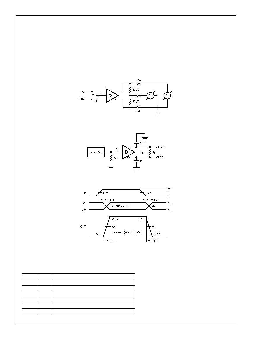
FIGURE 1. Differential Driver DC Test Circuit
DS100101-4
FIGURE 2. Differential Driver Propagation Delay and Transition Time Test Circuit
DS100101-5
FIGURE 3. Differential Driver Propagation Delay and Transition Time Waveforms
DS90L
V017A
www.national.com
3
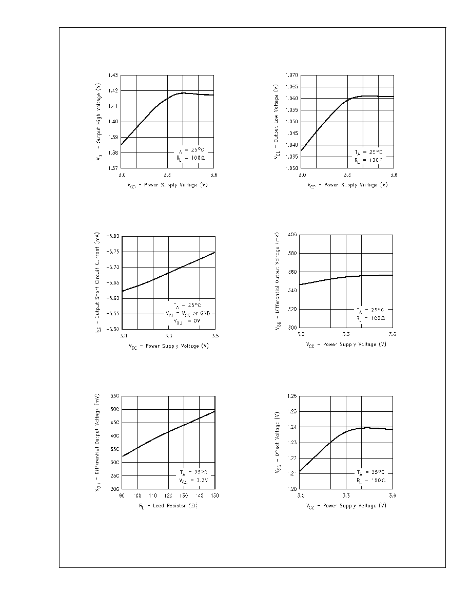
Typical Performance Curves
Output High Voltage vs
Power Supply Voltage
DS100101-7
Output Low Voltage vs
Power Supply Voltage
DS100101-8
Output Short Circuit Current vs
Power Supply Voltage
DS100101-9
Differential Output Voltage
vs Power Supply Voltage
DS100101-10
Differential Output Voltage
vs Load Resistor
DS100101-11
Offset Voltage vs
Power Supply Voltage
DS100101-12
DS90L
V017A
www.national.com
4
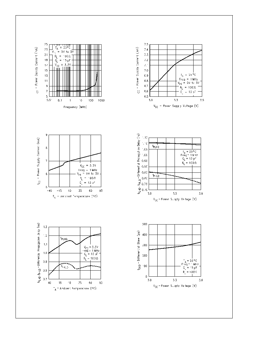
Typical Performance Curves
(Continued)
Power Supply Current
vs Frequency
DS100101-13
Power Supply Current vs
Power Supply Voltage
DS100101-14
Power Supply Current vs
Ambient Temperature
DS100101-15
Differential Propagation Delay vs
Power Supply Voltage
DS100101-16
Differential Propagation Delay vs
Ambient Temperature
DS100101-19
Differential Skew vs
Power Supply Voltage
DS100101-17
DS90L
V017A
www.national.com
5
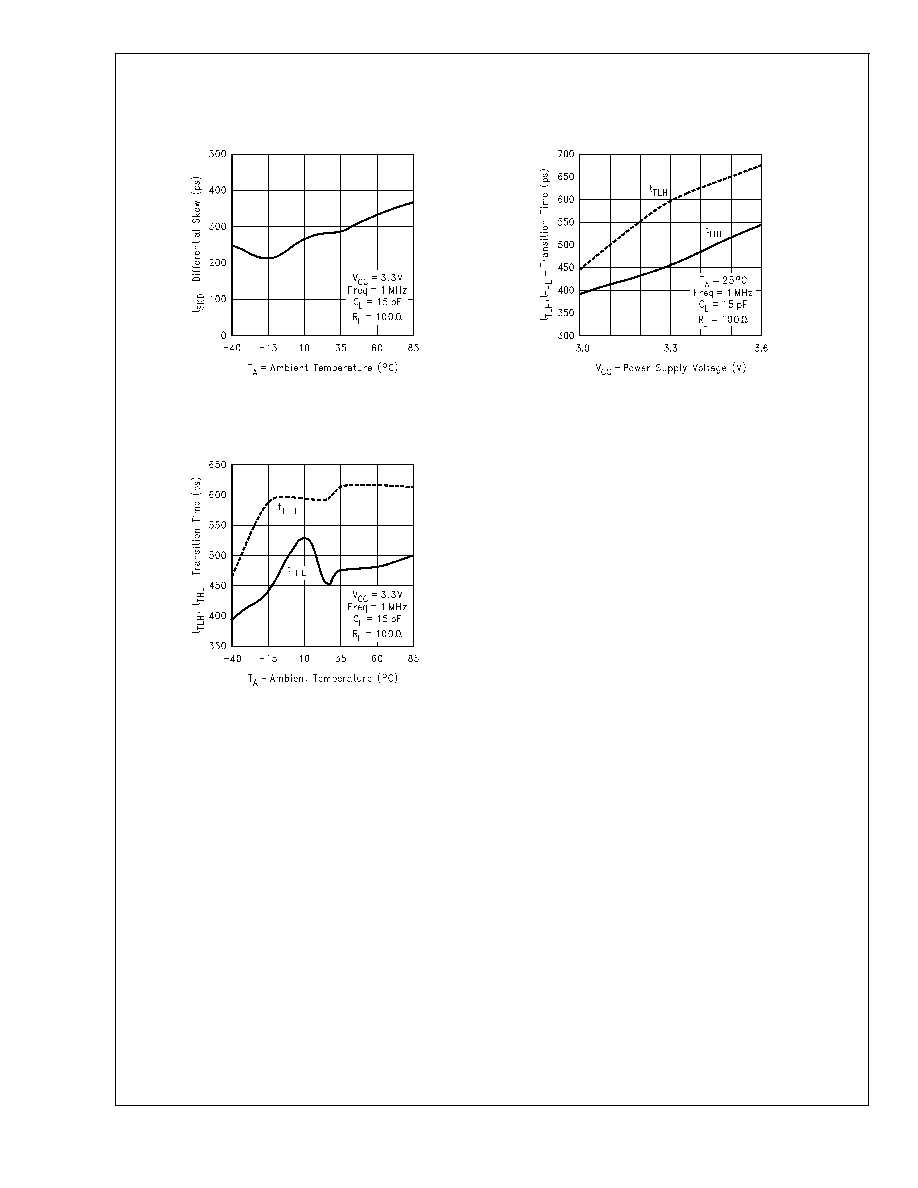
Typical Performance Curves
(Continued)
Differential Skew vs
Ambient Temperature
DS100101-20
Transition Time vs
Power Supply Voltage
DS100101-18
Transition Time vs
Ambient Temperature
DS100101-21
DS90L
V017A
www.national.com
6
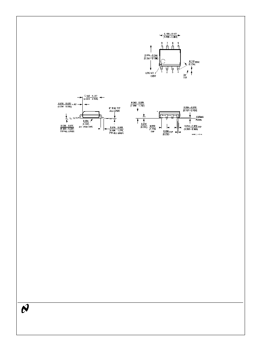
Physical Dimensions
inches (millimeters) unless otherwise noted
LIFE SUPPORT POLICY
NATIONAL'S PRODUCTS ARE NOT AUTHORIZED FOR USE AS CRITICAL COMPONENTS IN LIFE SUPPORT
DEVICES OR SYSTEMS WITHOUT THE EXPRESS WRITTEN APPROVAL OF THE PRESIDENT AND GENERAL
COUNSEL OF NATIONAL SEMICONDUCTOR CORPORATION. As used herein:
1. Life support devices or systems are devices or
systems which, (a) are intended for surgical implant
into the body, or (b) support or sustain life, and
whose failure to perform when properly used in
accordance with instructions for use provided in the
labeling, can be reasonably expected to result in a
significant injury to the user.
2. A critical component is any component of a life
support device or system whose failure to perform
can be reasonably expected to cause the failure of
the life support device or system, or to affect its
safety or effectiveness.
National Semiconductor
Corporation
Americas
Tel: 1-800-272-9959
Fax: 1-800-737-7018
Email: support@nsc.com
National Semiconductor
Europe
Fax: +49 (0) 180-530 85 86
Email: europe.support@nsc.com
Deutsch Tel: +49 (0) 69 9508 6208
English
Tel: +44 (0) 870 24 0 2171
FranÁais Tel: +33 (0) 1 41 91 8790
National Semiconductor
Asia Pacific Customer
Response Group
Tel: 65-2544466
Fax: 65-2504466
Email: ap.support@nsc.com
National Semiconductor
Japan Ltd.
Tel: 81-3-5639-7560
Fax: 81-3-5639-7507
www.national.com
Order Number DS90LV017ATM
NS Package Number M08A
DS90L
V017A
L
VDS
Single
High
Speed
Differential
Driver
National does not assume any responsibility for use of any circuitry described, no circuit patent licenses are implied and National reserves the right at any time without notice to change said circuitry and specifications.